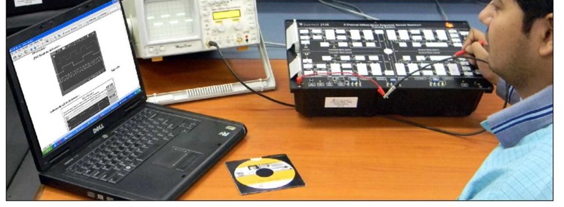
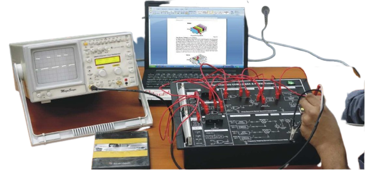
A2 CHANNEL CDMA – DSSS TRAINING SYSTEM

Technical Specifications:
Audio Section
Audio Input Section
Input Impedance : 600 ∧ (Microphone Socket)
Low pass Filter : 4th Order (3.4 KHz Cutoff)
Audio Output Section
Input impedance : 47 K∧ (Headphone Socket)
Headphone Socket : 3.5 mm stereo jack
Generator Section
Digitally Synthesized Sine & Cosine Wave Generator with frequency select 480KHz, 240KHz…8 & 16 bit digital data / pattern generator with frequency (68.6 KHz, 34.34 KHz….) & type (8 or 16 bit) select. Clock generator with frequency select 34.34 KHz, 68.6 KHz, 240 KHz, 480KHz, etc.
CDMA-DSSS Transmitter Section
Transmitter Clock : Bit Clock, Symbol Clock, and PN Clock: 68.6 KHz, 34.34 KHz & 240 KHz respectively
Delta Modulator : Comparator, Integrator, Unipolar to Bipolar converter, Variable sampling clock etc.
Bit Rate : 68.6 KHz, 34.34 KHz
Symbol Rate : 34.34 KHz, 17.17 KHz
PN-Code : 7 bit with select
Carrier : Sine & Cosine Wave
Modulation : QPSK Modulation
CDMA-DSSS Receiver Section
Receiver Clock Recovery : Bit Clock, Symbol Clock, and PN Clock: 68.6 KHz, 34.34 KHz & 240 KHz respectively
NCO : Sine & Cosine Wave.
Complex Multiplier : I & Q Channel
Integrator : I & Q Channel
Matched Filter & Correlator : I & Q Channel
Power Detector : I & Q Channel
Symbol Decoder : 34.34 KHz, 17.17 KHz.
Recovered Data : 68.6 KHz, 34.34 KHz
Delta-Demodulator: Variable clock, Unipolar to Bipolar Converter, Integrator, Low pass Filter, etc.
Learning material: CD (Theory, procedure, reference results, etc). Online (optional)
Multiple Access Section for Audio, internal data, external data mode.
Control Section
Controls bit clock, symbol clock, PN clock, PN code transmitter, PN code receiver, carrier clock, pattern length, software or hardware mode, experiment select.
Software Section
Real-time Software Section
Customized Graphical User Interface for specific experiment
Digital Signal Analysis
Analog Signal Analysis
Mixed Signal Analysis
XY Mode Analysis
Frequency Domain Analysis
Simulation Software Section
CDMA- Direct Sequence Spread Spectrum Transmitter Simulation
CDMA- Direct Sequence Spread Spectrum Receiver Simulation
CDMA Technical Document
Complete technical document of CDMA – Direct Sequence Spread Spectrum transmitter & receiver.
Power supply : 100 – 240V, ±10%, 50/60 Hz
Power consumption : 2.5VA approximately
Weight : 1.5Kg approximately
Dimension (mm) : W440×D265×H155
2 CHANNEL CDMA (DSSS & FHSS) TECHNIQUES

Simulation of Frequency Hopping (FH) system:
- Two Channel CDMA (DSSS and FHSS) is a comprehensive training solution for technology people, who want to explore the basics behind Code Division Multiple Access. The implementation of CDMA into practical life is so vast and intricate that it becomes really tough for beginners to get a feel of the real technology implementation.
aims to provide this feel of technology and gives necessary understanding of the CDMA multiplexing.
-
Features
- On-board data generators and PRN sequence generators
- BCD rotary switches for Data Selection
- Tap selectable PN sequence generators.
- Multiple data rate and chip rate selection
- Variable processing gain selection
- Slow and Fast frequency hopping demonstration.
- PN sequence driven Frequency synthesizer with non-overlapping frequency channel assignment.
- 2 Year Warranty
- Two Channel CDMA (DSSS and FHSS) Techniques comprises of following major blocks:
- Direct Sequence Spread Spectrum based CDMA.
- Data generators
- PN sequence generators.
- DSSS modulators and Multiplexer
- DSSS demodulator (Integrate and dump filter)
- Variable data rate chip rate selection.
- Numeric display for transmitted and received data.
- Frequency Hoping Spread Spectrum based CDMA:
- Data generators
- PN sequence generators.
- Frequency synthesizers
- FHSS modulators and Multiplexer
- FHSS demodulator
- Numeric display for transmitted and received data.
CONVOLUTION (ENCODER & DECODER) (2122a & 2122b)

Objectives:
- Techbooks are compact and user friendly learning platforms to provide a modern, portable, comprehensive and practical way to learn TechnologTo observe the changes in carrier centre frequency and to observe the frequency deviation, and to observe how the phase lock loop can be used for FM demodulation.
- Techbooks 2122A and 2122B Convolution encoder and decoder are designed to provide Conceptual and Step by Step understanding of Convolution codes. Block wise modulator organization of circuit functions with Code tree, State and Trellis Diagram makes it easy to understand, the process of encoding and decoding. Additional onboard redundant bit generator is provided so that user can insert error to generated code and decode error free data.
-
Features:
- Convolution encoder.
- Selectable rate:
- N = 3, rates ½; N = 7, rate ¾
- Manual and Continuous mode operation.
- Encoder Code tree
- On – board data and clock generation
- On – board error generation.
- Convolution decoder
- Selectable rate:
- = 3, rates ½; N = 7, rate ¾
- State and Trellis diagram.
- Support hard decision and soft decision decoding.
- Decoded data bit display.
- Single supply.
- 2 year warranty.
.
Scope of learning:
- Study of Convolution Encoding and code tree of encoder for N = 3 with rate = ½
- Study of Decoder with state and Trellis Diagram for N = 3 with rate = ½
- Study of Convolution Encoding and Decoding with error
- Study of Convolution Encoding using Puncturing for N = 7 and rate = ¾
- Study of Soft decision Viterbi Decoding using Depuncturing for N = 7 with rate = ¾
- Technical specifications:
- Word length : 4 bits.
- Selectable rate : ½ and ¾
- Data format : NRZ (Not Return to Zero)
- Interconnections : 2 mm sockets (Gold Plated)
- Test points : Gold plated.
- Power supply : 100 – 240V AC, 50/60 Hz
- Operating condition : 0 - 40ºC, 85% RH
- Internal Power supply : +5V DC
- Dimensions (mm) : 326W×252D×52H
- Weight : 1.5Kgs. (approximately)
- Learning material : Online (Theory, procedure, reference results, etc)
- Included accessories : Patch cord 16”10 Nos
- Power supply for 2122A & 2122B – 1 No each
- Mains cord – 2Nos
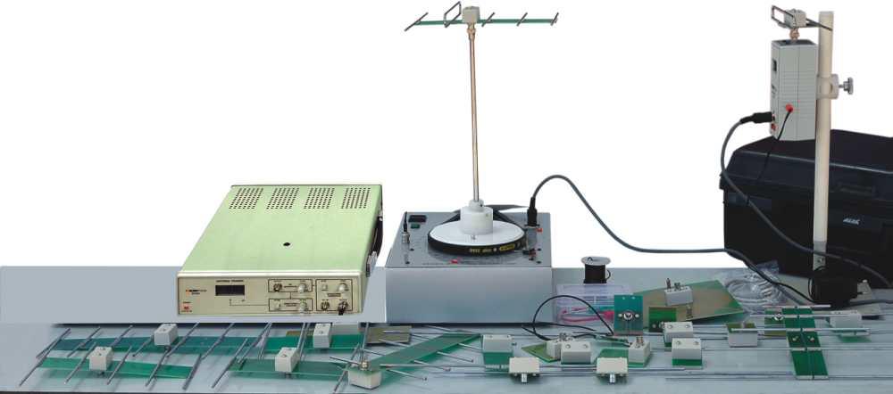
MOTORISED ANTENNA UNIT (2261)

FEATURES:
-
- Microcontroller Based Precision DC Stepper Motor
- Automatic Zero Point setting
- Built-in DC Power Supply
- Instant Plotting of radiation Pattern
- Resolution : 1º
- RS232 data link to PC
- Software running under Windows 98, XP, and Windows 7.0 Version
- 2 year warranty
.
TECHNICAL SPECIFICATIONS
-
- RF input : From
- Detector : Active with 5 pin DIN
- Connector
- Power supply : 220/110V, 50Hz/60Hz on request
- Power consumption : 2VA (approximately)
- Dimensions(mm) : W285×D390×H88
- Weight : 3Kg(approx.)]
- Accessories : Mains Cord, 5 pin DIN cable, Patch cords, BNC-BNC Cable, RS232 Cable, Radiation Pattern Plotting Software.
- Learning material : CD (Theory, procedure reference results, etc.). Online (optional)
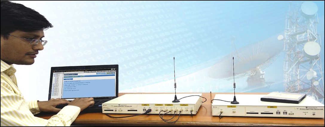
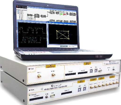
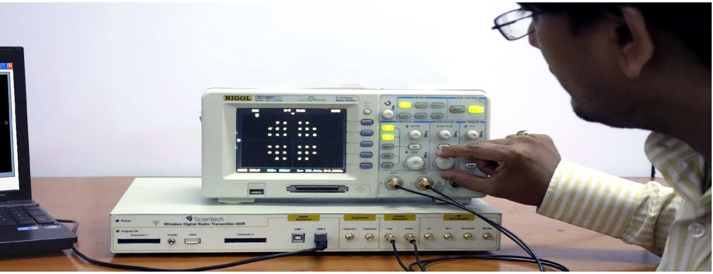
WIRELESS DIGITAL RADIO –SDR

FEATURES:
-
- Software Radios represent a major change in the design paradigm for radios in which a large portion of the functionality is implemented through programmable signal processing devices, giving the radio the ability to change its operating parameters to accommodate new features and capabilities. A Software Radio approach reduces the content of Radio Frequency (RF) and other analog components of traditional radios and emphasizes Digital Signal Processing to enhance overall receiver flexibility. Software Radios are emerging in commercial and military infrastructure. This growth is motivated by the numerous advantages of Software Radios like ease of design, ease of manufacture, Multimode operation, use of advanced signal processing techniques, fewer discrete components, flexibility to incorporate additional functionality, etc. Given these clear advantages and the increasing processing power available in commercial Digital Signal Processing devices, we are confident that Software Radios will become the standard approach for radio design. Wireless Digital Radio-SDR is a complete solution to learn & develop concepts of Software Radio in a real time environment. User can study and design all the building block of Software Radio like baseband and RF sections.
- FEATURES:
- Portable design
- Block level study and implementation
- USB2.0 interface
- User programmable
- Interactive Software for various Labs.
- Internal & External data mode
- Baseband signal study of I & Q
- Dual 125 MSPS 10-bit D/A converters for I Channel and Q Channel.
- Control setting for individual blocks
- Built-in RF-up converter
- Built in RF-down converter
- Provision for external reference signal for PLL
- Gold plated SMA connectors
- Built-in analog signal acquisition
- Logic Analyzer for digital signal analysis
- Constellation view for I & Q
- Study of impairments
- Digital Filters: Interpolation, Decimation and Raised Root Cosine with variable roll-off (a).
- Various Spreading codes
- Built-in low-noise frequency synthesizer
- Variable chip rate up to 10 Mchips/s.
- JTAG USB connector for FPGA configuration
- 2 Year Warranty
- To study the fundamentals and frequency domain measurement of Spectrum Analyzer
- To study the Un-modulated carrier for SDR-Transmitter by applying different signals like constant data / sine wave / cosine wave at I channel and Q channel
- To study about baseband signals and band-pass signals
- To examine rectangular pulse, its bandwidth and frequency spectrum
- To study the concept of Pulse Shaping to improve Spectral Efficiency
- To compare the performance of sine-shaped & rectangular pulses
- Study about Roll-off factor (a)
- To study about Information Capacity, Bit-rate, Symbol Rate and M- ary encoding
- To study and analyze BPSK modulation in time & frequency domain and its constellation view
- To study and analyze DBPSK modulation in time & frequency domain and its constellation view
- To study and analyze DQPSK modulation in time & frequency domain and its constellation view
WIRELESS DIGITAL RADIO –SDR

WIRELESS DIGITAL RADIO –SDR:
- To study and analyze OQPSK modulation in time & frequency domain and its constellation view
MSK Constellation
- To study and analyze p/4-QPSK modulation in time & frequency domain and its constellation view
32-APSK Constellation
- To study and analyze p/4-DQPSK modulation in time & frequency domain and its constellation view
- To study and analyze MSK modulation in time & frequency domain and its constellation view
- To study and analyze 8-PSK modulation in time & frequency domain and its constellation view
- To study and analyze 8-QAM modulation in time & frequency domain and its constellation view
16-APSK Constellation
- To study and analyze 16-PSK modulation in time & frequency domain and its constellation view
8-QAM Constellation
- To study and analyze 16-QAM modulation in time & frequency domain and its constellation view
- To study and analyze 16-APSK modulation in time & frequency domain and its constellation view
- To study and analyze 32-QAM modulation in time & frequency domain and its constellation view
- 64 -QAM Constellation
- To study and analyze 64-QAM modulation in time & frequency domain and its constellation view
32-QAM Constellation
- To study and analyze 128-QAM modulation in time & frequency domain and its constellation view
- To study about Interpolation Factor, Interpolation Low Pass Filter
- To study about Decimation Factor, Decimation Low Pass Filter, Digital
- 16-PSK Constellation
- To study about Direct Sequence Spread Spectrum System(DSSS), PN codes, types of PN codes, Chip Rate, Spreading Factor, Processing Gain
- To study about Single Carrier Transmitter, Multi Carrier Transmitter
- To study and analyze OFDM modulation, Sub-carriers, Symbol Rate, Bandwidth Efficiency
- 16-QAM Constellation
- To study and analyze Convolution Encoder, Interleaver and De-interleaver
Wireless Digital Radio Transmitter –SDR

SPECIFICATIONS:
- Maximum Data Rate: 10 Mbps
- Device Xilinx FPGA Spartan3E XC3S500E
- Dual 125 MSPS 10-bit D/A converters for I Channel and Q Channel
- 6-pole Butterworth clock rejection filters
- Maximum bandwidth: +/- 13 MHz @±0.4dB ripple
- DAC clock rejection @40 MHz > 84 dBc
-
- Output voltage: 1Vpp with 0.85V DC bias
-
- JTAG USB connector for FPGA configuration
- Standard built-in Modulations like BPSK, DBPSK, QPSK, OQPSK, DQPSK, П/4 QPSK, П/4DQPSK, MSK, 8PSK, 8QAM, 16PSK, 16QAM, 16APSK, 32QAM, 32APSK, 64QAM, 128QAM
- Multilevel Signal
- Digital Filters: Interpolation, Decimation and Raised Root Cosine with variable roll-off (α)
- Interactive Software with USB 2.0 interface for various Labs
-
- Internal Data Generator as test pattern
- Programmable chip rates up to 10 Mchip/s
- Spreading codes:
- 23 - Gold sequences (up to 2 chips)
- 23 - Maximal length sequences, (max length 2 chips)
- Barker codes (length 11, 13)
- Dual-band (902-928 MHz) or (2.025 - 2.5GHz), quadrature modulator,
- Low-noise frequency synthesizer can be tuned over entire range by steps of 100, 31.25 or 25 KHz
- 8 preset frequencies for fast (<2ms) local oscillator frequency tuning
- MSK Modulation
- Selectable internal / external 10 MHz frequency reference for the frequency synthesizer
- Gold platted SMA(F) connectors for Base-band and RF
- Built-in channel impairments generation: AWGN and Frequency Offset (Doppler)
- Data Acquisition Section: (for both Transmitter & Receiver)
- Analog Channel: 2 (CH1 & CH2)
- Resolution: 8-bit
- Digital Channel: 8 (D0 – D7)
- Maximum Real-time Sampling: 100MSPS (Analog + Digital Channel Simultaneously)
- Memory Depth: 2K
- Mode: Y-T (Time-domain View) & X-Y (Constellation View)
- Interactive GUI with USB2.0 Interface
- Wireless Digital Radio Receiver –SDR
Wireless Digital Radio Receiver –SDR

SPECIFICATIONS:
- Maximum output data rate: 10 Mbps
- Device Xilinx FPGA Spartan3E XC3S500E
- Dual 10-bit Analog-to-Digital converters, 40 Msamples/s
- Selectable internal 40 MHz / external ADC sampling clock (to synchronize multiple receivers)
- Baseband filtering options: Wideband applications (< 26 MHz)
- JTAG USB Connector for FPGA configuration
- Interactive Software with USB 2.0 interface for various Labs
- Dual-band, [902-928 MHz] and (2.025 – 2.5 GHz) receiver
- 128-QAM Constellation
- Sensitivity: -56 dBm RF input for full scale 10-bit output samples
- Built-in RF AGC, 70 dB dynamic range
- Low phase-noise frequency synthesizer can be tuned over entire range by steps of 100, 31.25, or 25 KHz
- 8 preset frequencies for fast (<2ms) local oscillator frequency tuning
- Selectable internal / external 10 MHz frequency reference for the frequency synthesizer
- SMA connectors
- Direct Sequence Spread-Spectrum demodulator
- Variable chip rate up to 10 Mchips/s
- 32-APSK Constellation
-
- Spreading codes:
- Gold sequences (up to 223 chips)
- Maximal length sequences, (max length 223 chips)
- Barker codes (length 11, 13)
- BPSK, QPSK selectable
- Demodulation performances: within 1.5 dB from theory at threshold SNR of 5 dB
- Sequential code search
- Receiver lock monitoring using software
- External Digital Interface connector for expansion
- Measures actual bit errors while a known PRBS-11 pseudo-random test sequence is being transmitted


